Motherboard


The most important circuit board of a computer system is called the motherboard (also mainboard, system board, logic board).
It contains the most important electronic components of a computer system such as processor, graphics chip, ROM and RAM. It also includes internal and external interfaces for connecting additional peripherals.
The C64 Motherboards[edit | edit source]
The first motherboard for the C64 was released in August 1982. Over the course of the C64's production run (until 1993), several revisions of the motherboards were released for the purpose of cost optimization, bug fixes, and efficiency improvements. Rare individual cases of prototypes built at a very early development stage sometimes have no version printed on the board. Boards without revision information are also known from the ASSY 326298-01.
In addition to the following versions/revisions, there are various prototype boards.
1982: ASSY 326298[edit | edit source]

- Schematic: 326106
- Known revisions: 6, A, B, C
- Some specimens exist without revision numbers
- Some earlier revisions were still used in prototypes
- Most have the 5-pin audio/video output (i.e., without separate chroma signal); however, revisions with 8-pin connector also exist
- Commodore designation: Original
Details see #ASSY 326298-01.
1982: KU-14194HB[edit | edit source]

- Fab No.: 251022
- Does not carry an Assy No., but is identified by the community based on the board material number for distinction. The same material was also used for some VC-20 motherboards, which also have the same imprint, but here additionally with an Assy No.
- Not mentioned in the known (American) service manuals and was therefore presumably only sold in Europe
- This and all subsequent motherboards fundamentally have the 8-pin audio/video output
- Known revisions: A, B
Details see #KU14194HB.
1983: ASSY 250407[edit | edit source]

Custom Character ROM

- Fab No.: 250406; Artwork No.: 251137; Schematic: 251138
- Known revisions: A, B, C
- Commodore designation: A (CR)
Details see #ASSY 250407-01.
1984: ASSY 250425[edit | edit source]

(Version without protection diodes)

(Version with protection diodes)
- Schematic: 251469; P/N: 251470-01
- Known revisions: A, B
- Commodore designation: B
Details see #ASSY 250425.
1986: ASSY 250466[edit | edit source]

- Schematic: 252278; P/N: 252280-01
- Known revisions: A
- Commodore designation: B-3
Details see #ASSY 250466.
1987: ASSY 250469[edit | edit source]
 (Without SID) |
 (Without SID and without VIC) |
 |
 |
 (Version for the C64GS) |
- PCB No.: 252311; Schematic: 252312
- Known revisions: 1, 3, 4, A, B
- Commodore designation: E
Details see #ASSY 250469.
Differences by Television Standard[edit | edit source]
There are PAL and NTSC models of all boards.
Although it is not clearly visible from the labeling on most ASSY boards, they differ by the version of the VIC-II, the oscillator, and a data line on the board.
On the 250469 boards, the designation -10 or -09 for PAL or NTSC is also printed after the ASSY number.
No separate boards were manufactured for the SECAM television standard; such computers were modified after the fact. SECAM C64s were available, for example, in France as pre-modified retail units, or alternatively one could purchase the board separately for conversion and install it in a PAL computer. In a similar way, a C64 could also be converted to RGB (using Procep RGB), after which the television standard was no longer relevant.
The C64 Games System was only manufactured as a PAL version, as it was sold exclusively in the United Kingdom.
Additional Devices[edit | edit source]

(A Max Machine board)
In Commodore documents (Service Manual), an ASSY 250441 (B-2) is mentioned. It is said to differ electrically from the 250425 only in having a few layout changes. Since no specimen has ever been sighted, it is assumed that it never made it to market.
SX64[edit | edit source]
On the SX64, the ASSY number was not printed on the board, but it is documented:
- 1983: ASSY 250408-01
Max Machine[edit | edit source]
The Commodore MAX Machine only came with one board version, which differs in many ways from a proper C64:
- 1982: ASSY 325565
- Known revisions: A, B
C64 Golden Edition[edit | edit source]

In the golden C64, which were given away in Germany in 1987 on the occasion of one million units sold, an ordinary ASSY 250407-01 is installed.
The Golden Edition differs from a normal breadbin solely due to its special case.
C64 Aldi[edit | edit source]

The C64 Aldi has a completely ordinary ASSY 250469 board, usually revision 3. However, due to several erroneous reports in the magazine 64'er, the rumor persists that the Aldi computers received their own, cost-reduced board. Supposedly, the 9V power supply on the user port is missing. But that is simply false.
C64GS[edit | edit source]
The game console C64GS uses a slightly modified form factor of the ASSY 250469 and largely corresponds in technical internals to the normal C64 home computers. The then-current, final revision B was always used. Differences include the expansion port rotated 90 degrees upward, as well as the absence of the keyboard connector and serial port. The C64 Games System also has its own KERNAL/BASIC ROM. Since this board does not offer any new developments or improvements, it is not an independent revision.
PET 64/CBM 4064[edit | edit source]
The PET 64/CBM 4064 used an ordinary ASSY 326298, frequently in revision A.
The C64 Motherboards in Detail[edit | edit source]
ASSY 326298-01[edit | edit source]
The "original" C64 computers shown at the Winter Consumer Electronics Show in Las Vegas in 1982 had the motherboard ASSY 326298-01 with revision 6.[2]. These C64s are classified as prototypes, but the motherboard revision can still be found occasionally. Such boards were usually still populated with ceramic chips.
- 5-pin motherboard (CN5 video port or connector has 5 pins).
- PCB (Printed Circuit Board) number 326298-01.
Schematics[edit | edit source]
Schematic number 326106 [2] [3] [4]
![[2]](https://www.zimmers.net/anonftp/pub/cbm/schematics/computers/c64/326106-1of2.gif)
![[3]](https://www.zimmers.net/anonftp/pub/cbm/schematics/computers/c64/326106-2of2.gif)
Parts List[edit | edit source]
According to excerpt from the parts list[3][4]
ICs[edit | edit source]
| Ref. | P/N | Description |
|---|---|---|
| U1, U2 | 6526 | CIA |
| U3 | 2364 | ROM (BASIC) |
| U4 | 2364 | ROM (KERNAL) |
| U5 | 2364 | ROM (Character Set) |
| U6 | 2114L-30 | SRAM 1024x4 Bit (Color RAM) |
| U7 | 6510 | Processor |
| U8 | 7406 | Hex Inverter (Open Collector) |
| U9-U12 | 4164 | DRAM 64Kx1 (200 ns). U9=Data bit 1, U10=D3, U11=D5, U12=D7. |
| U13 | 74LS257 | Quad 2-line to 1-line Data selector/Multiplexer, Non-inverting Outputs |
| U14 | 74LS258 | Quad 2-line to 1-line Data selector/Multiplexer, Inverting Outputs |
| U15 | 74LS139 | Dual 2 to 4-line Decoder/Demultiplexer, Inverting Outputs |
| U16 | 4066 | Quad Analog Switch |
| U17 | 82S100 | PLA |
| U18 | 6581 | SID |
| U19 | 6567 | VIC II |
| U20 | LM556 | Dual Timer |
| U21-U24 | 4164 | DRAM 64Kx1 Bit (200 ns). U21=Data bit 0, U22=D2, U23=D4, U24=D6. |
| U25 | 74LS257 | Quad 2-line to 1-line Data selector/Multiplexer, Non-inverting Outputs |
| U26 | 74LS373 | Octal Transparent Latch |
| U27 | 74LS08 | Quad 2-input AND-Gate |
| U28 | 4066 | Quad Analog Switch |
| U29 | 74LS74 | Dual D-positive Edge Triggered Flip-flop, Asynchronous Preset and Clear |
| U30 | 74LS193 | Synchronous presettable up/down 4-bit Binary Counter, Clear |
| U31 | 74LS629 | Dual Voltage-controlled Oscillator, Enable control, Range control |
| U32 | MC4044 | Phase-frequency Detector |
Diodes[edit | edit source]
| Ref. | P/N | Description |
|---|---|---|
| CR1 | 1N4371 | Zener 2.7 V, 500 mW |
| CR2 | 1N755 | Zener 7.5 V, 500 mW |
| CR3 | 1N914 | Diode |
| CR4 | Varo VM08 | Bridge Rectifier, 2 A/100 V |
| CR5, CR6 | 1N4001 | Diode 1 A/60 V |
Transistors[edit | edit source]
| Ref. | P/N | Description |
|---|---|---|
| Q1 | 2N4401 | NPN Small Signal |
| Q2 | 2N3904 | NPN Small Signal |
| Q3 | TIP29B | NPN Power |
| Q4-Q8 | 2N2222 | NPN Small Signal |
KU14194HB[edit | edit source]
This board was only used briefly and was soon replaced by the 250407. It is quite rare to find.
It was installed almost exclusively in PAL versions.
ASSY 250407-01[edit | edit source]
Schematics[edit | edit source]
![[6]](https://www.zimmers.net/anonftp/pub/cbm/schematics/computers/c64/251138-1of2-combined.gif)
![[7]](https://www.zimmers.net/anonftp/pub/cbm/schematics/computers/c64/251138-2of2-combined.gif)
Parts List[edit | edit source]
Excerpt from the parts list[5][6]
ICs[edit | edit source]
| Ref. | P/N | Description |
|---|---|---|
| U1, U2 | 6526 | CIA |
| U3 | 2364 | ROM (BASIC) |
| U4 | 2364 | ROM (KERNAL) |
| U5 | 2332 | ROM (Character Set) |
| U6 | 2114L-20 | SRAM 1024x4 Bit (Color RAM) |
| U7 | 6510 | Processor |
| U8 | 7406 | Hex Inverter (Open Collector) |
| U9-U12 | 4164 | DRAM 64Kx1 Bit (200 ns). U9=Data bit 1, U10=D3, U11=D5, U12=D7. |
| U13 | 74LS257 | Quad 2-line to 1-line Data selector/Multiplexer, Non-inverting Outputs |
| U14 | 74LS258 | Quad 2-line to 1-line Data selector/Multiplexer, Inverting Outputs |
| U15 | 74LS139 | Dual 2 to 4-line Decoder/Demultiplexer, Inverting Outputs |
| U16 | 4066 | Quad Analog Switch |
| U17 | 82S100 | PLA |
| U18 | 6581 | SID |
| U19 | 6567 | VIC II |
| U20 | LM556 | Dual Timer |
| U21-U24 | 4164 | DRAM 64Kx1 Bit (200 ns). U21=Data bit 0, U22=D2, U23=D4, U24=D6. |
| U25 | 74LS257 | Quad 2-line to 1-line Data selector/Multiplexer, Non-inverting Outputs |
| U26 | 74LS373 | Octal Transparent Latch |
| U27 | 74LS08 | Quad 2-input AND-Gate |
| U28 | 4066 | Quad Analog Switch |
| U29 | 74LS74 | Dual D-positive Edge triggered Flip-flop, Asynchronous Preset and Clear |
| U30 | 74LS193 | Synchronous Presettable Up/down 4-bit Binary Counter, Clear |
| U31 | 74LS629 | Dual Voltage-controlled Oscillator, Enable control, Range control |
| U32 | MC4044 | Phase-frequency Detector |
Diodes[edit | edit source]
| Ref. | P/N | Description |
|---|---|---|
| CR1 | 1N4371 | Zener 2.7 V, 500 mW |
| CR2 | 1N755 | Zener 7.5 V, 500 mW |
| CR4 | S2VB10 Sub: DBA20B Sub: DBA20C |
Bridge Rectifier, 2 A/100 V |
| CR5, CR6 | 1N4001 | Diode 1 A/60 V |
Transistors[edit | edit source]
| Ref. | P/N | Description |
|---|---|---|
| Q1, Q2 | 2SC1815 | NPN Small Signal |
| Q3 | TIP29A | NPN Power |
| Q7, Q8 | 2SC1815 | NPN Small Signal |
ASSY 250425[edit | edit source]
This revision replaced the clock generation circuit using a single IC (U31, 8701).
Schematics[edit | edit source]
![[10]](https://www.zimmers.net/anonftp/pub/cbm/schematics/computers/c64/251469-1of2.gif)
![[11]](https://www.zimmers.net/anonftp/pub/cbm/schematics/computers/c64/251469-2of2.gif)
Parts List[edit | edit source]
Excerpt from the parts list[7][8]
ICs[edit | edit source]
| Ref. | P/N | Description |
|---|---|---|
| U1, U2 | 6526 | CIA |
| U3 | 2364 | ROM (BASIC) |
| U4 | 2364 | ROM (KERNAL) |
| U5 | 2332 | ROM (Character Set) |
| U6 | 2114L-20 | SRAM 1024x4 Bit (Color RAM) |
| U7 | 6510 | Processor |
| U8 | 7406 | Hex Inverter (Open Collector) |
| U9-U12 | 4164 | DRAM 64kx1 (200 ns). U9=Data bit 1, U10=D3, U11=D5, U12=D7. |
| U13 | 74LS257 | Quad 2-line to 1-line Data selector/Multiplexer, Non-inverting Outputs |
| U14 | 74LS258 | Quad 2-line to 1-line Data selector/Multiplexer, Inverting Outputs |
| U15 | 74LS139 | Dual 2 to 4-line Decoder/Demultiplexer, Inverting Outputs |
| U16 | 4066 | Quad Analog Switch |
| U17 | 82S100 | PLA |
| U18 | 6581 | SID |
| U19 | 6567 | VIC II |
| U20 | LM556 | Dual Timer |
| U21-U24 | 4164 | DRAM 64Kx1 (200 ns). U21=Data bit 0, U22=D2, U23=D4, U24=D6. |
| U25 | 74LS257 | Quad 2-line to 1-line Data selector/Multiplexer, Non-inverting Outputs |
| U26 | 74LS373 | Octal Transparent Latch |
| U27 | 74LS08 | Quad 2-input AND-Gate |
| U28 | 4066 | Quad Analog Switch |
| U31 | 7701/8701 | Clock Generator |
Diodes[edit | edit source]
| Ref. | P/N | Description |
|---|---|---|
| CR1 | 1N4371 | Zener 2.7 V, 500 mW |
| CR2 | 1N754A | Zener 6.8 V, 500 mW |
| CR4 | S2VB10 Sub: DBA20B Sub: DBA20C Sub: DBA20C-K15 |
Bridge Rectifier, 2 A/100 V |
| CR5, CR6 | 1N4001 | Diode 1 A/60 V |
| CR100-105 (CR9, CR12-CR16) |
1N4148 Sub: 1N914 |
Diode |
Note: CR100 - 105 are protection diodes for the IEC bus, which in later versions of ASSY # 250425 were soldered onto other components ("piggybacked").
Transistors[edit | edit source]
| Ref. | P/N | Description |
|---|---|---|
| Q1 | TIP29A | NPN Power |
| Q2-Q4 | 2SC1815 | NPN Small Signal |
ASSY 250441-01[edit | edit source]
A Commodore employee stated about the motherboard ASSY 250441-01 that it has the same trace layout as the ASSY 250425, with only a few small parts changed. Allegedly, a few models were already distributed.
![[13]](https://www.zimmers.net/anonftp/pub/cbm/schematics/computers/c64/251138-sheet1of2.gif)
![[14]](https://www.zimmers.net/anonftp/pub/cbm/schematics/computers/c64/251138-sheet2of2.gif)
Commodore C64/C64C Service Manual (PN-314001-03, March 1992), Page 17:
Version B-2, 8 pin board (Reduced Osc. w/component changes), PCB ASSY # 250441-01*, Schematics 251469
[...]
* The 4th version of 64 board was recently developed and only a few may be in the field. It is termed the 64B-2. All circuits remain the same as 64B (Schematic 251469) with a few component location changes:
1) Resistors 28, 29, 30, 36, 48 were reduced to Resistor Pack RP5.

2) Diodes CR100-105 are no longer piggybacked. Their new locations are CR9, 12-16.

Nevertheless, to this day there is no evidence of the actual existence of this ASSY. There are no further statements about it, and no photos or schematics. Since the listed changes were minimal, it is questionable why Commodore should have assigned a new ASSY number for this. Realistically, it would at best have been designated as a new revision of the 250425.
On the other hand, one must not forget that previously unknown boards have surfaced several times. If the 250441-01 does exist, the model probably only exists as an NTSC version.
Parts List[edit | edit source]
According to the description, the parts should largely match a 250425 board.
ASSY 250466[edit | edit source]
Rarer than the 250407 and 250425 is the ASSY 250466. It was mainly installed in the first C64C cases. On this board, the eight 8KB RAM chips were replaced by two 32KB RAM chips. A VIC-II 6569 Rev.5 was usually installed. The SID 6581-R4AR was also typical here.
Schematics[edit | edit source]
![[16]](https://www.zimmers.net/anonftp/pub/cbm/schematics/computers/c64/252278-1.gif)
![[17]](https://www.zimmers.net/anonftp/pub/cbm/schematics/computers/c64/252278-2.gif)
Parts List[edit | edit source]
According to excerpt from the parts list[9][10]
ICs[edit | edit source]
| Ref. | P/N | Description |
|---|---|---|
| U1, U2 | 6526 or 8521 | CIA |
| U3 | 2364B-161 | ROM (BASIC) |
| U4 | 2364B-273 | ROM (KERNAL) |
| U5 | 2332C-250 | ROM (Character Set) |
| U6 | 2114 | SRAM 1Kx4 Bit (200 ns) |
| U7 | 6510 | Processor |
| U8 | 7406 Sub: 7416 |
Hex Inverter (Open Collector) |
| U9, U10 | 50464-150 | DRAM 64Kx4 Bit (150 ns). U9: Data bits 4-7, U10: Data bits 0-3. |
| U13 | 74LS257A | Quad 2-line to 1-line Data selector/Multiplexer, Non-inverting Outputs |
| U14 | 74LS258A | Quad 2-line to 1-line Data selector/Multiplexer, Inverting Outputs |
| U15 | 74LS139 | Dual 2 to 4-line Decoder/Demultiplexer, Inverting Outputs |
| U16 | 4066B | Quad Analog Switch |
| U17 | 82S100 | PLA 8700-001 |
| U18 | 6581 R3 | SID |
| U19 | 6567 | VIC NTSC |
| U20 | NE556 | Dual Timer |
| U25 | 74LS257A | Quad 2-line to 1-line Data selector/Multiplexer, Non-inverting Outputs |
| U26 | 74LS373 | Octal Transparent Latch |
| U27 | 74LS08 | Quad 2-input AND-gate |
| U28 | 4066B | Quad Analog Switch |
| U31 | 8701T6 Sub: 8701L6 |
Clock Generator |
Diodes[edit | edit source]
| Ref. | P/N | Description |
|---|---|---|
| CR1 | 1N4371 | Zener 2.7 V, 500 mW |
| CR2 | 1N754A | Zener 6.8 V, 500 mW |
| CR4 | S2VB10 Sub: DBA20B Sub: DBA20C Sub: DBA20C-K15 |
Bridge Rectifier, 2 A/100 V |
| CR5, CR6 | 1N4001 | Diode 1 A/60 V |
| CR9, CR12-CR16 | 1N4148 Sub: 1N914 |
Diode |
Transistors[edit | edit source]
| Ref. | P/N | Description |
|---|---|---|
| Q1 | 2SD880 Sub: TIP29A Sub: 2SD476 Sub: 2SD313 Sub: 2SD1310 Sub: 2SD1266 |
NPN Power |
| Q2-Q4 | 2SC1815 Sub: 2SC945 Sub: 2SC2458 Sub: 2SC2785 |
NPN Small Signal |
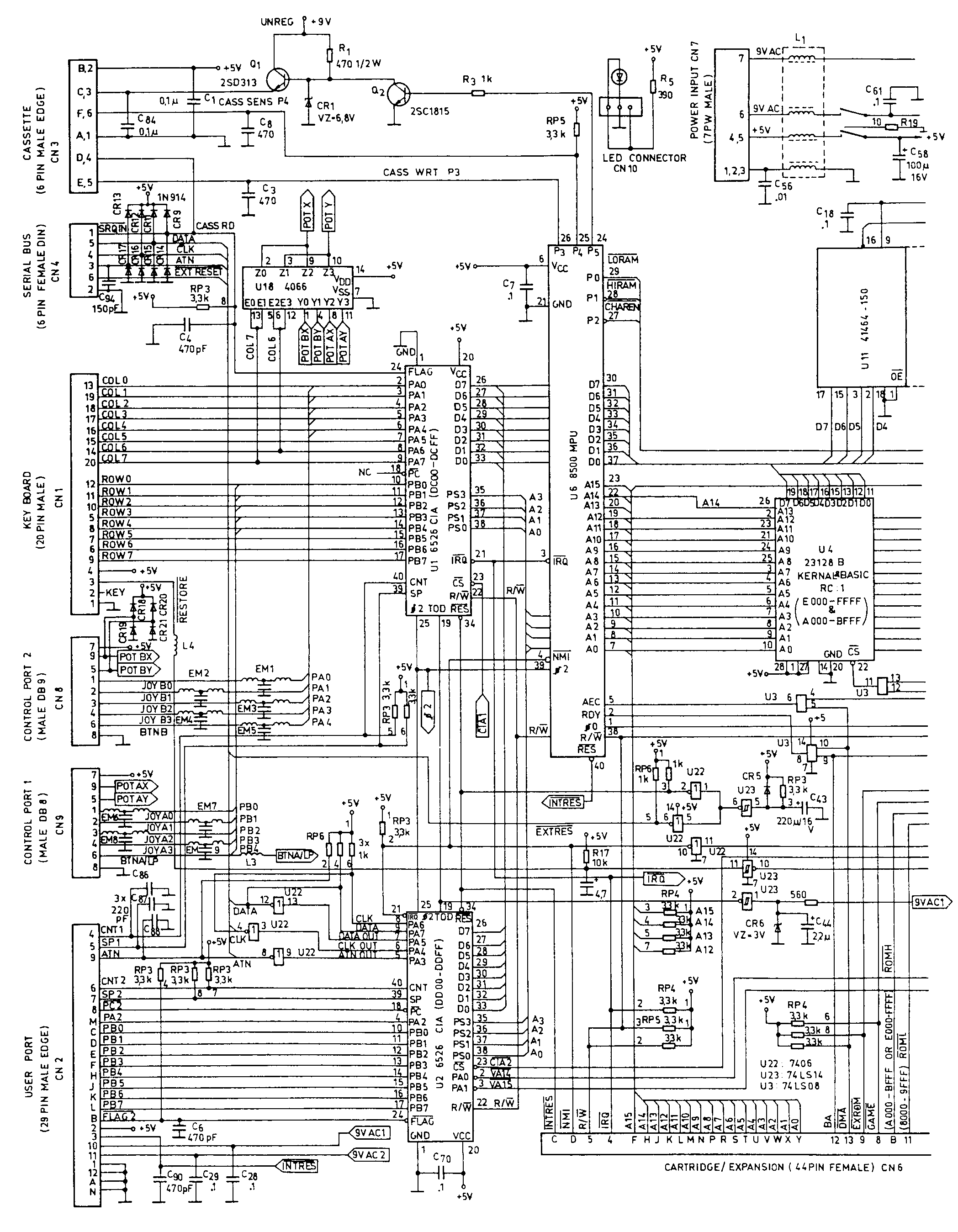
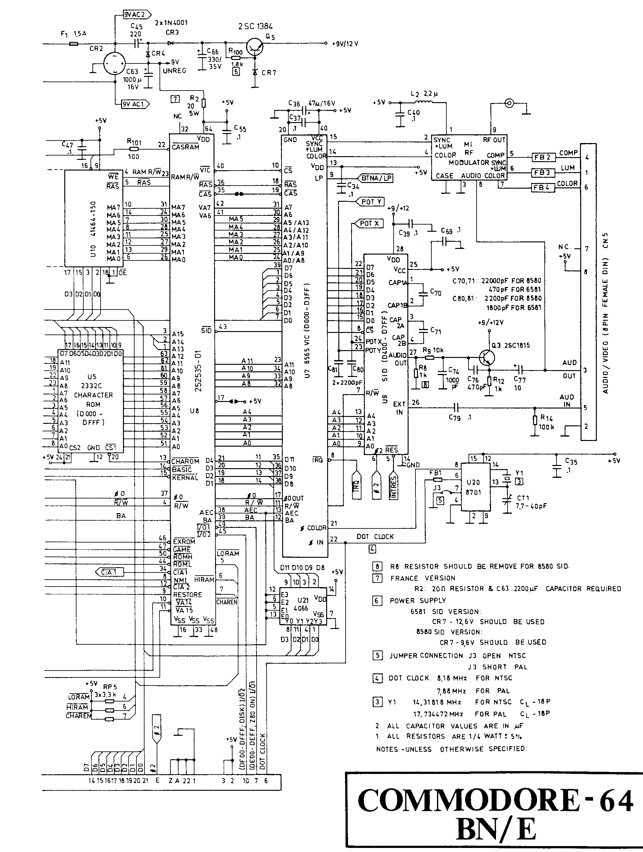
ASSY 250469[edit | edit source]
The 250469 was the last version of the C64 board. Since this board has a narrower design compared to its predecessors, it is colloquially referred to as the "short board".
- PLA and some additional circuits were integrated into a multifunction chip with 64 pins, with the final revision B also including the color RAM.[11]
- As with the 250466, only 2 RAM ICs with 32 KB each were installed.
- Typically, the HMOS variants of the VIC-II and SID were installed, which run at lower supply voltage than the older NMOS variants. The chips therefore cannot simply be swapped between board variants.
- The second 5V rail including its 5V voltage regulator was eliminated; the 250469 has only one 5V rail, which is fed directly from the power supply's 5V.
- The 9V/12V for the SID are no longer generated via voltage regulator, but via a transistor circuit.
Revisions 3, 4, A and especially B are very common.[12] Revision 1, on the other hand, is a very rare board, and no specimen of revision 2 has been found yet.
Behind the ASSY number, the suffix -10 for PAL or -09 for NTSC computers was often printed.
Schematics[edit | edit source]
- Schematics on zimmers.net
- Left part (both revisions), right part for Rev. A and right part for Rev. B
- These should be taken with a grain of salt, especially the one for Rev. B contains some inconsistencies - essentially only the missing color RAM was "drawn in". The further changes (see below) are not entered at all.
- Replica by bwack on github.com
- Interactive BOM and Layout: [19]
Comparison of Revisions[edit | edit source]
Common Features:
- Common to all 250469 revisions is the strong cost optimization, e.g., through a combined KERNAL/BASIC ROM and through a custom IC. This combines almost all the TTL logic of the old boards (multiplexers, etc.) and the functions of the "old" PLAs (906114) in a single 64-pin IC. It will be referred to here as the "64-Pin Custom IC".
- Likewise, in contrast to earlier boards, all 250469 revisions use only one 5V rail.
- Also, all known versions are populated with HMOS-II ICs (8500, 8565, 8580, ...).
Differences:[13]
- U8 - 64-Pin Custom IC
- Rev. 1, 3, 4 and A have the 64-Pin Custom IC "251715-01" - no integrated color RAM.
- Rev. B has the 64-Pin Custom IC "252535-01" - integrated color RAM and various other small changes:
- The chip select for the BASIC and KERNAL ROM was combined and now appears on Pin 15. With this, Commodore obviously decided not to use two separate chips for BASIC and KERNAL ROM anymore (with extra logic to connect A14 with the CS signal it would still be possible: When accessing the KERNAL, A14 is high, when accessing BASIC the line is low, easily implementable for example with half a 74LS139).
- To integrate the CHAR ROM with the BASIC/KERNAL ROM, Pin 48 of the 64-Pin Custom IC 252535-01 serves for switching. Then only a single combined chip select for BASIC, CHAR and KERNAL ROM is generated.
Pin 48 can be switched either to Vcc or to GND using two solder jumpers (J15, J16). The default configuration on Rev. B is to GND.
- U19 - Color RAM, 2114, 1024 x 4 Bit
- Present on Rev. 1, 3, 4, A.
- Not present on Rev. B, but integrated into the 64-Pin Custom IC.
- U3 - TTL, 74LS08, quad AND-gate
- Rev. 1 - Status unknown.
- Rev. 3 and 4
- U3a - Not used (pins open!).
- U3b - Generates AEC signal for CPU from VIC-AEC and DMA from Expansion Port.
- U3c - Generates RDY signal for CPU from VIC-BA and DMA from Expansion Port.
- U3d - Generates CS for the combined BASIC/KERNAL ROM from the lines BASIC (U8, Pin 14) and KERNAL (U8, Pin 15) of the 64-Pin Custom IC.
- Rev. A
- U3a - The inputs are connected in parallel, the gate acts as a simple driver stage; "DOTCLOCK" from U20 (8701), Pin 6 is fed to the input, the output goes to the VIC (U7), Pin 22. This is a change introduced with Rev. A; previous revisions do not have this driver stage, there the 8701 is connected directly to the VIC.
- U3b - Generates AEC signal for CPU from VIC-AEC and DMA from Expansion Port.
- U3c - Generates RDY signal for CPU from VIC-BA and DMA from Expansion Port.
- U3d - Generates CS for the combined BASIC/KERNAL ROM from the lines BASIC (U8, Pin 14) and KERNAL (U8, Pin 15) of the 64-Pin Custom IC.
No gate of U3 is free anymore.
- Rev. B
- U3a - The inputs are connected in parallel, the gate acts as a simple driver stage; "DOTCLOCK" from U20 (8701), Pin 6 is fed to the input, the output goes to the VIC (U7), Pin 22. This is a change introduced with Rev. A; previous revisions do not have this driver stage, there the 8701 is connected directly to the VIC.
- U3b - Generates AEC signal for CPU from VIC-AEC and DMA from Expansion Port.
- U3c - Generates RDY signal for CPU from VIC-BA and DMA from Expansion Port.
- U3d - Not used.
Solder Jumpers:
| Solder Jumper | Default | Pad 1 - Connected to | Pad 2 - Connected to | Explanation |
|---|---|---|---|---|
| J10 | open | 64-Pin Custom IC Pin 14 (BASIC) | J11+J10 (second side) and BASIC-KERNAL ROM Pin 1 (A15) and 27 (A14) | Supplies A14 for the ROM in special operating mode. |
| J11 | closed | Vcc | J10+J11 (second side) and BASIC-KERNAL ROM Pin 1 (A15) and 27 (A14) | Sets Pins 1 and 27 of the ROM to Vcc in normal operation with 27C128. |
| J12 | closed | J13 and BASIC-KERNAL ROM Pin 26 (A13!) | CPU A14 | Supplies CPU/A14 as A13 for BASIC-KERNAL ROM in normal mode (separate CHAR ROM). |
| J13 | open | J12 and BASIC-KERNAL ROM Pin 26 (A13!) | 64-Pin Custom IC Pin 13 (CHAR) | When closed and J12 open, the 64-Pin Custom IC supplies A13 for the combined BASIC-KERNAL-CHAR ROM. |
| J14 | closed | CHAR ROM Pin 20 (CS) | 64-Pin Custom IC Pin 13 (CHAR) | Supplies CS for CHAR ROM with separate IC. |
| J15 | closed | 64-Pin Custom IC Pin 48 | GND | Normal operating mode with separate CHAR ROM. |
| J16 | open | 64-Pin Custom IC Pin 48 | Vcc | Special operating mode with a single combined ROM. |
| J18 | open | 64-Pin Custom IC Pin 17 | Vcc | Has the connection designation COLORRAM. If J18 is not closed, the screen remains dark. |
Using a single EPROM for BASIC/KERNAL/CHAR[edit | edit source]
Commodore planned to replace the three/two ROM chips by a single one apparently. For the 252535-01, this is possible using the following steps.
- The combined BASIC-KERNAL-CHAR ROM must presumably be a 23256 (with a 27C256 EPROM, Pin 1 must be bent up and connected to Vcc, since Pin 1 is Vpp and is connected to Pin 27 on the board).
- Disconnect J12, this separates A13 from the BASIC-KERNAL ROM (Pin 26) from CPU A14.
- Close J13, this makes the 64-Pin Custom IC supply A13 for the combined BASIC-KERNAL-CHAR ROM (Pin 26).
- Disconnect J14, this separates the chip select for the CHAR ROM.
- Close J10, supplies A14 for the combined BASIC-KERNAL-CHAR ROM (Pin 27).
- Disconnect J11, so that Pins 1 and 27 of the BASIC-KERNAL-CHAR ROM are not permanently connected to Vcc.
- Disconnect J15, close J16, this connects Pin 48 of the 64-Pin Custom IC to Vcc instead of GND and the ROM operating mode should (presumably) be switched.
- Install a properly programmed 32 KB ROM (23256) (will be rather hard to find) or properly program a 27C256 EPROM and bend Pin 1 up and clamp it to Vcc.
- The 27C256 EPROM would have to be programmed as follows:
- $0000 ... $1FFF - empty (unused, could also be used for your favorite cartridge)
- $2000 ... $3FFF - BASIC ROM
- $4000 ... $4FFF - empty (unused)
- $5000 ... $5FFF - CHAR ROM
- $6000 ... $7FFF - KERNAL ROM
- The ROM thus simply covers the upper 32 KB range, whereby it only "shines through" at those points where the CS signal enables it. The corresponding ROM content can be found in the associated source [14]. Because this allocation corresponds to the C64 address range of $8000-$FFFF, this saves the complex decoding and the EPROM can be connected practically 1:1 with the address bus.
- The 27C256 EPROM would have to be programmed as follows:
So that the CHAR ROM in the combined EPROM at $5000 to $5FFF can also be addressed by the VIC (which expects it from its perspective at $1000..$1FFF), the 64-Pin Custom IC supplies a modified A13 (J12=open, J13=closed: Pin 13 thus supplies "A13mod"). Internally, this is achieved by AND-ing A13 from the address bus with CS of the CHAR ROM. Thus:
| CS of the CHAR ROM | A13mod |
|---|---|
| 1 | A13 |
| 0 | 0 |
Parts List[edit | edit source]
Excerpt from the parts list[15][16]
ICs[edit | edit source]
| Ref. | P/N | Description |
|---|---|---|
| U1, U2 | 6526 | CIA |
| U3 | 74LS08 | Quad 2-input AND gate |
| U4 | 23128B | ROM US PAL 251913 |
| U5 | 2332C | ROM CHAR US PAL 901225 |
| U6 | 8500 | CPU |
| U7 | 8565: PAL 8562: NTSC |
VIC-II |
| U8 | 251715-01 or 252535-01 | Memory Controller/PLA (252535 includes color RAM/former U19) |
| U9 | 8580 | SID |
| U10 | 41464-150 | DRAM 64k x 4 (Data bits 0-3) |
| U11 | 41464-150 | DRAM 64k x 4 (Data bits 4-7) |
| U18 | 4066 | Quad Analog Switch |
| U19 | 2114 | SRAM 1024x4 Bit, 901453 (200 ns) |
| U20 | 8701T6 | Clock Generator |
| U21 | 4066 | Quad Analog Switch |
| U22 | 7406 Sub: 7416 |
Hex Inverter (Open Collector) |
| U23 | 74LS14 | Hex Inverter (Schmitt-trigger) |
Diodes[edit | edit source]
| Ref. | P/N | Description |
|---|---|---|
| CR1 | RD6.8EB Sub: 1N754A |
Zener 6.8 V, 500 mW |
| CR2 | S2VB10 Sub: DBA20B Sub: DBA20C |
Bridge Rectifier 100 V/2 A |
| CR3,4 | 1N4001 | Diode |
| CR5,9,11-21 | 1N914 Sub 1N4148 |
Diode |
| CR6 | RD3.0EB1 Sub: RD3.0FB2 |
Zener 3.16-3.38 V, 500 mW |
| CR7 | RD10ESB2 Sub: RD13ESB2 Sub: HZ11A1 Sub: HZ12B2 |
Zener, 10 V, 500 mW |
Transistors[edit | edit source]
| Ref. | P/N | Description |
|---|---|---|
| Q1 | 2SD880 Sub: TIP29A Sub: 2SD476AC Sub: 2SD313E/F Sub: 2SD1310 |
NPN |
| Q2,3 | 2SC1815 Sub: 2SC945 Sub: 2SC2458 |
NPN |
| Q5 | 2SC1384 | NPN |
Capacitors[edit | edit source]
Note: The parts list in the service manual for the 250469 board is incorrect. The capacitor value for the RESTORE key function is correct in the schematic, but wrong in the parts list.[17]
See Also[edit | edit source]
Sources[edit | edit source]
- ↑ Service Manual C64/C64C PN-314001-03 (March 1992), Page 3
- ↑ archive.org copy from March 3, 2016 of the page http://www.vintage.org/special/2003/c64prototype C64 Prototypes
- ↑ Service Manual C64/C64C PN-314001-03, Page 19
- ↑ Circuit diagram 326106
- ↑ Service Manual C64/C64C PN-314001-03, Page 24
- ↑ Circuit diagram 251138
- ↑ Service Manual C64/C64C PN-314001-03, Page 29
- ↑ Circuit diagram 251469
- ↑ Service Manual C64/C64C PN-314001-03, Page 34
- ↑ Circuit diagram 252278
- ↑ [1]
 translation: On the ASSY 250469 Rev.3, Rev.4 and Rev.A, you can find the color RAM with the label "MN2114-2" or "LC3514A-15" right next to the 64-pin hybrid chip "251715-01".
- ↑ Thread: ASSY 250469 Revisions? on Forum64.de
- ↑ Author of the analyses on ASSY 250469: User kinzi from Forum64
- ↑ Thread: ASSY 250469 Revisions? on Forum64.de 32K ROM image of the ASSY-250469 board
- ↑ Service Manual C64/C64C PN-314001-03, Page 40
- ↑ Circuit diagram 252312
- ↑ Thread: Schematic for 250469 board wrong? on Forum64.de
External Links[edit | edit source]
| Wikipedia: Motherboard |