PLA (C64 chip)

The Programmable Logic Array (PLA) derives its name from the Signetics 82S100 bipolar tri-state one-time field-programmable logic array that was built into the earliest of Commodore 64s. Later models manufactured by MOS Technology, a subsidiary of Commodore, or Commodore Semiconductor Group (CSG) were not available as programmable variants but instead came readily mask-programmed from the factory in NMOS technology. This chip in the C64 only contains combinatorial logic. The MOS/CSG versions are fully pin-compatible with the original Signetics IC which has 16 input lines, 8 output lines and allows for 48 Product ("AND") terms.
Designed by Dave DiOrio, the PLA is used to create chip select signals received from various other signals. These signals control which chip is to be connected to the data bus. Therefore the PLA is responsible for dictating the memory map of the C64 and enables the implementation of bank switching. Commodore engineer James Redfield said it was the "glue logic to tie everything together". The final version of the PLA logic was REV3, before it was superseded on Assy 250469 motherboards by the 251715-01 SuperPLA (still with external 2114 for 4x1K bits static video color RAM) and later the 252535-01 "Memory Controller W/ SRAM" which integrates the PLA, the 4x1K bits static video color RAM and various 74xx TTL series ICs.
In the VICE x64sc C64 emulator, there is a switch to choose between the old PLA and "discrete" glue logic or the 251715-01/252535-1 glue logic on IC which has slightly different timing characteristics. The new variants may cause the VIC-II to fetch wrong data in rare corner cases. This is by all means negligible in practice and only of theoretical or academic interest, mostly for demo sceners.
This original PLA chip is failure prone, especially the earliest models. Eventually, third party PLAs were created, such as the SuperPLA, realPLA, U17 PLAnkton, PLAtinum, neatPLA, PLA20V8 (aka "GAL-PLA") and also PLAs based on eproms as a replacement part. Timing is critical for proper compatibility, possibly mainboard components need to be adjusted especially if the replacement part switches "too fast" in comparison to the original PLA. "Wrong" timing may only ever show when using certain cartridges.
Pinout[edit | edit source]

| Pin | Name | Remarks |
|---|---|---|
| 1 | FE/NC | Used for programming field-programmable parts and not connected internally for mask programmable parts.[1] |
| 2 | I7 | Connected to A13 of the address bus |
| 3 | I6 | Connected to A14 of the address bus |
| 4 | I5 | Connected to A15 of the address bus |
| 5 | I4 | Connected to #VA14 on VIC-II |
| 6 | I3 | Connected to #CHAREN on I/O port of the 6510 CPU |
| 7 | I2 | Connected to #HIRAM on I/O port of the 6510 CPU |
| 8 | I1 | Connected to #LORAM on I/O port of the 6510 CPU |
| 9 | I0 | Connected to #CAS on the VIC-II |
| 10 | F7 | #ROMH |
| 11 | F6 | #ROML |
| 12 | F5 | #I/O |
| 13 | F4 | GR/#W, connected to #WE on the color RAM |
| 14 | VSS | GND |
| 15 | F3 | Connected to #CS1 on the #CHAROM |
| 16 | F2 | Connected to #CS on the #KERNAL ROM |
| 17 | F1 | Connected to #CS on the #BASIC ROM |
| 18 | F0 | #CASRAM, connected to the #CAS pin on the DRAM |
| 19 | #CE | Chip Enable |
| 20 | I15 | Connected to VA12 on VIC-II |
| 21 | I14 | Connected to VA13 on VIC-II |
| 22 | I13 | Connected to #GAME on pin 8 of cartridge port |
| 23 | I12 | Connected #EXROM on pin 9 of cartridge port |
| 24 | I11 | Connected to R/#W of the bus |
| 25 | I10 | #AEC, connected to inverted version of AEC on the VIC-II |
| 26 | I9 | Connected to BA on the VIC-II |
| 27 | I8 | Connected to A12 of the address bus |
| 28 | VCC | +5V |
Links[edit | edit source]
- Giesel, Thomas: "The C64 PLA Dissected"; accessed 24 October 2013
- pla.txt
 - PLA circuit logic for old 82S100-PLAs at zimmers.net
 - PLA signal matrix
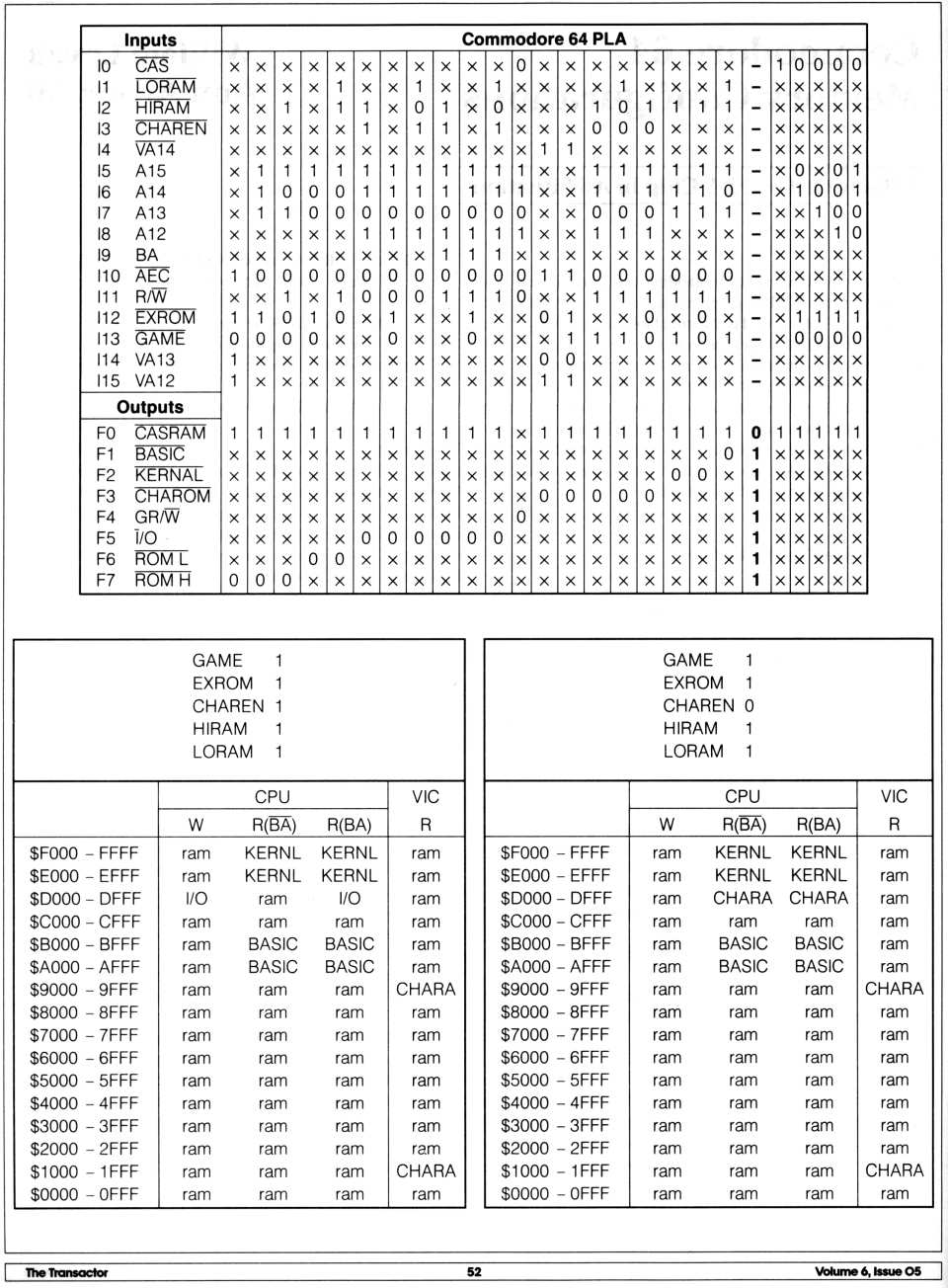
- PLA signal matrix explanation from The Transactor Volume 6, Issue 05, pp. 51,