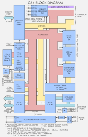
Block Diagram of the Motherboard
[2]The C64 motherboard (also mainboard, system board, logic board) is a double-sided PCB (Printed Circuit Board) featuring conductive tracks etched from copper sheets laminated onto a non-conductive substrate. The motherboard features electronic components (CPU, ROM, RAM etc) embedded directly into the substrate or seated in embedded sockets as well as connectors and interfaces for internal and external peripherals. Component identifier labels are over-printed on the PCB. Together, the boards and components are referred to as a PCBA (Printed Circuit Board Assembly). The C64 motherboard operates on TTL (Transistor-Transistor Logic), uses a composite system bus for communications and many of its components are IC chips dedicated to individual tasks.
C64 motherboards first appeared for retail in August 1982; and although they displayed the year and revision number, the year was soon omitted. In order to improve efficiency and reduce costs, designs were frequently revised. It is important to note then that there is no intended correlation between the chronological development of PCBs, components and cases. Although there may be some pattern setting during the assembly runs, this cannot be relied upon to date a motherboard. An inspection of the PCB must me made if certainty of motherboard type is required. Additionally, there were many C64s returned to Commodore for repair, and motherboards were replaced with what was available; with the replaced board likely to feature in the repair of another C64. In short, nothing should be inferred about the lineage of a motherboard.
- 5-pin board (CN5-Video port has 5 pins).
- PCB Number 326298-01.
- Schematic Number 326106.
- The machines on display at the 1982 Winter Consumer Electronics Show in Las Vegas were Rev 6 boards [3]. These machines were still classed as prototypes, and so it is unlikely that previous revisions will be found.
- These early machines had many ceramic chips.
| PCB Identifier
|
Code
|
Remarks
|
|
PCB Identifier
|
Code
|
Remarks
|
|
PCB Identifier
|
Code
|
Remarks
|
|
PCB Identifier
|
Code
|
Remarks
|
| U1 |
6526 |
CIA 1
|
U2 |
6526 |
CIA 2
|
U3 |
2364 |
ROM (BASIC)
|
U4 |
2364 |
ROM (KERNAL)
|
| U5 |
2332 |
ROM (Character)
|
U6 |
2114L-30 |
SRAM
|
U7 |
6510 |
Processor
|
U8 |
7406 |
Logic NOT (Hex Inverter)
|
| U9 |
4164 |
RAM
|
U10 |
4164 |
RAM
|
U11 |
4164 |
RAM
|
U12 |
4164 |
RAM
|
| U13 |
74LS257 |
Multiplexor
|
U14 |
74LS258 |
Multiplexor
|
U15 |
74LS139 |
Demultiplexor
|
U16 |
4066 |
Quad Bilateral Switch
|
| U17 |
82S100 |
PLA
|
U18 |
6581 |
SID
|
U19 |
6567 |
VIC-II
|
U20 |
LM556 |
Dual Timer
|
| U21 |
4164 |
RAM
|
U22 |
4164 |
RAM
|
U23 |
4164 |
RAM
|
U24 |
4164 |
RAM
|
| U25 |
74LS257 |
Multiplexor
|
U26 |
74LS373 |
Multiplexor
|
U27 |
74LS08 |
Logic AND
|
U28 |
4066 |
Quad Bilateral Switch
|
| U29 |
74LS74 |
Logic NOR (Divider)
|
U30 |
74LS193 |
Binary Counter
|
U31 |
74LS629 |
Oscillator
|
U32 |
MC4044 |
Logic (Phase Detector)
|
| PCB Assembly Diagram
|
PCB Schematic
|
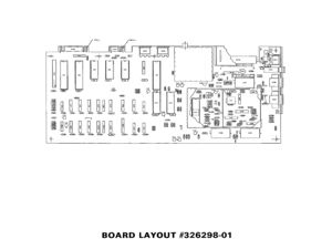 PCB Assembly Number 326298-01 |
|
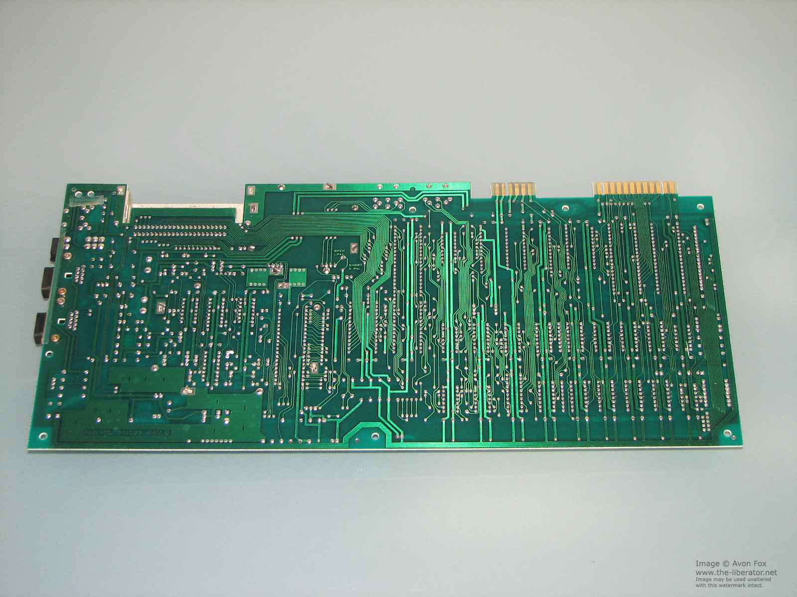
- PCB Assembly Number KU-14194HB.
- Schematic Number 251022.
- The KU-14194HB was the first C64 board with separate Y/C video signals.
- It is a PAL only board.
- Revision number on rear of PCB.
| PCB Assembly Diagram
|
PCB Schematic
|
 PCB Assembly Number KU14194 |
|
- 8-pin board (CN5-Video port has 8 pins).
- PCB Assembly Number 250407-04.
- Schematic Number 251138.
| PCB Identifier
|
Code
|
Remarks
|
|
PCB Identifier
|
Code
|
Remarks
|
|
PCB Identifier
|
Code
|
Remarks
|
|
PCB Identifier
|
Code
|
Remarks
|
| U1 |
6526 |
CIA 1
|
U2 |
6526 |
CIA 2
|
U3 |
2364 |
ROM (BASIC)
|
U4 |
2364 |
ROM (KERNAL)
|
| U5 |
2332 |
ROM (Character)
|
U6 |
2114L-30 |
SRAM
|
U7 |
6510 |
Processor
|
U8 |
7406/7416 |
Logic NOT (Hex Inverter)
|
| U9 |
4164 |
RAM
|
U10 |
4164 |
RAM
|
U11 |
4164 |
RAM
|
U12 |
4164 |
RAM
|
| U13 |
74LS257 |
Multiplexor
|
U14 |
74LS258 |
Multiplexor
|
U15 |
74LS139 |
Demultiplexor
|
U16 |
4066 |
Quad Bilateral Switch
|
| U17 |
82S100 |
PLA
|
U18 |
6581 |
SID
|
U19 |
6567 |
VIC-II
|
U20 |
LM556 |
Dual Timer
|
| U21 |
4164 |
RAM
|
U22 |
4164 |
RAM
|
U23 |
4164 |
RAM
|
U24 |
4164 |
RAM
|
| U25 |
74LS257 |
Multiplexor
|
U26 |
74LS373 |
Multiplexor
|
U27 |
74LS08 |
Logic AND
|
U28 |
4066 |
Quad Bilateral Switch
|
| U29 |
74LS74 |
Logic NOR (Divider)
|
U30 |
74LS193 |
Binary Counter
|
U31 |
74LS629 |
Oscillator
|
U32 |
MC4044 |
Logic (Phase Detector)
|
| PCB Assembly Diagram
|
PCB Schematic
|
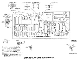 PCB Assembly Number 250407-04 |
|
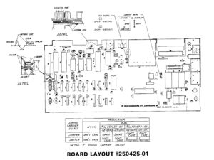
- 8-pin board (reduced oscillator circuit).
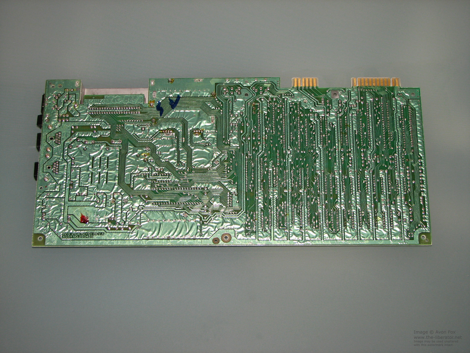
- PCB Assembly Number 250425-01.
- Schematic Number 251469.
- CIAs, ROMs, CPU, SID, PLA, and VIC may be all socketed.
| PCB Assembly Diagram
|
PCB Schematic
|
 PCB Assembly Number 250425-01 |
|
- 8-pin board (reduced oscillator with component changes).
- PCB Assembly Number 240441-01.
- Schematic Number 251469.
- All circuits remain the same as the C64B (Schematic 251469) with a few component location changes.
- Resistors 28, 29, 30, 36 and 48 were reduced to Resistor Pack RP5.
- Diodes CR100-15 are no longer piggy-backed. Their locations are CR9, CR12-16.
| PCB Assembly Diagram
|
PCB Schematic
|
PCB Assembly Number 240441-01 |
|
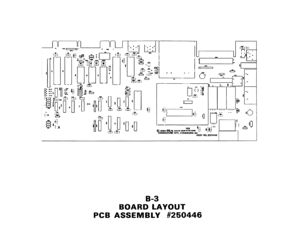
- Only 2 RAM chips, U9, U10.
- PCB Assembly Number 250466.
- Schematic Number 252278.
- In 1986, Commodore released the last revision to the classic C64 motherboard. It was otherwise identical to the 1984 design, except for the two 64 kilobit × 4 bit DRAM chips that replaced the original eight 64 kilobit × 1 bit ICs.
- After the release of the C64C, MOS Technology began to reconfigure the C64's chipset to use HMOS production technology. The main benefit of using HMOS was that it required less current to drive the IC, which consequently generates less heat. This enhanced the overall reliability of the SID and VIC-II. The new chipset was renumbered to 85xx to reflect the change to HMOS.
- The modifications to the C64 line were more than skin deep in the C64C with new versions of the SID chips being deployed—with the core voltage reduced from 12 V to 9 V, and the VIC using only 5V. The I/O chips remained functionally identical but the new 8521 which uses HMOS technology uses about half the power of the original NMOS 6526. The basic and kernal 2364 ROMs were also replaced with a single 23128 ROM.
| PCB Assembly Diagram
|
PCB Schematic
|
 PCB Assembly Number 250466 |
|
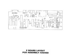
- PCB Assembly Number 250469.
- Schematic Number 252311, 252312
- KERNAL & BASIC ROMS combined into U4.
- New IC memory controller, U8.
- In 1987, Commodore released C64Cs with a highly redesigned motherboard commonly known as a "short board".
- The "short board" used the new HMOS chipset, featuring a new 64-pin PLA chip. The new "SuperPLA", as it was dubbed, integrated many discrete components and Transistor–Transistor Logic (TTL) chips.
- In the last revision of the C64C motherboard, the 2114 color RAM was integrated into the SuperPLA.
| PCB Assembly Diagram
|
PCB Schematic
|
 PCB Assembly Number 250469 |
|
|
- ↑ http://www.vintage.org/special/2003/c64prototype, accessed 1 November 2013
- ↑ Service Manual C64/C64C PN-314001-03 (March 1992), Page 3
- ↑ http://www.vintage.org/special/2003/c64prototype, accessed 1 November 2013
- ↑ http://www.c-64.org/de/mainboards.html, accessed 31 October 2013
- ↑ http://www.classic-videogames.de/?p=494, accessed 30 October 2013
- ↑ http://c64preservation.com/dp.php?pg=registry, accessed 31 October 2013
- ↑ https://gona.mactar.hu/Commodore/C64/C64_PCB_AssyKU-14194RevA_-_best_quality.jpg
- ↑ http://the-liberator.net/site-files/retro-games/hardware/Commodore-64/Commodore-64-Brown-Compare-UK-GER/Commodore-64-Brown-German-REV-B-011-Motherboard.JPG
- ↑ http://c64preservation.com/dp.php?pg=registry, accessed 31 October 2013
- ↑ http://www.mos6502.com/commodore-tech-corner/commodore%E2%80%99s-inner-space-%E2%80%93-revolutions, accessed 30 October 2013
- ↑ http://www.old-computers.com/museum/computer.asp?c=98&st=1, accessed 25 October 2013
- ↑ http://the-liberator.net/site-files/retro-games/hardware/Commodore-64/Commodore-64-Brown-Compare-UK-GER/Commodore-64-Brown-England-REV-A-009-Motherboard.JPG
- ↑ http://c64preservation.com/dp.php?pg=registry, accessed 31 October 2013
- ↑ http://c64preservation.com/dp.php?pg=registry, accessed 31 October 2013
- ↑ http://ilesj.wordpress.com, ilesj's blog, accessed 30 October 2013


